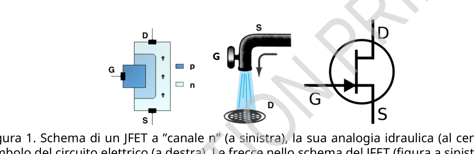
Experiment Q1-1 Italian (Italy) Transistor di carta (10 punti) La tecnologia elettronica nella società moderna si basa su un dispositivo semplice ma potente: il transistor, che può essere utilizzato sia come interruttore che come amplificatore. In modalità interruttore il transistor viene utilizzato per la memorizzazione e l’elaborazione di informazioni digitali. Qui analizzeremo due tipi di transistor a effetto di campo (FET = Field Effect Transistor): il JFET (transistor a effetto di campo di giunzione) e il TFT (transistor a campo sottile). Spieghiamo brevemente come funziona un FET. Un FET è un dispositivo non lineare a 3 terminali [i terminali sono chiamati Base (Gate G); emettitore (Source S);collettore (Drain D)] che può controllare il flusso di corrente tra Source e Drain agendo sulla tensione applicata tra Gate e Source . In un’analogia semplice, benché imperfetta, un FET funziona in modo simile a un rubinetto dell’acqua, dove la manopola che controlla il flusso dell’acqua svolge un ruolo analogo al Gate. Figura 1. Schema di un JFET a ”canale n” (a sinistra), la sua analogia idraulica (al centro) e il simbolo del circuito elettrico (a destra). Le frecce nello schema del JFET (figura a sinistra) indicano il flusso della corrente elettrica tra Source (S) e Drain (D) attraverso lo stretto ”canale n”. La larghezza del canale dipende dalla tensione applicata tra Gate (G) e Source (S). Il Junction-FET (JFET) funziona grazie alle proprietà della giunzione (del contatto) tra due tipi di un materiale semiconduttore, come il silicio drogato p e n. Per questo motivo viene chiamato ”Junction”-FET. Un JFET contiene uno stretto canale attraverso il quale scorre la corrente tra Source e Drain, e in un FET a ”canale n” questo canale è fatto di materiale di tipo n. La larghezza di questo canale può essere controllata in modo preciso applicando una tensione negativa tra Gate e Source, VGS= . Per VGSfissato, la corrente che scorre tra Source e Drain dipende in maniera non lineare dalla tensione applicata tra Drain e Source, VDS= . Tuttavia, se la tensione VDSè piccola, la corrente dipende in modo lineare dalla tensione applicata, pertanto il JFET segue la legge di Ohm. Tuttavia, la resistenza di uscita, RDS= VDS IDS dipende fortemente dalla tensione VGSapplicata, e segue con ottima approssimazione la legge: RDS = R0 DS 1 , (1) dove R0 DSè la resistenza di uscita per VGS= 0 e VP< 0 è un parametro relativo al JFET chiamato la tensione di pinch-off. Chiaramente, alla tensione di pinch-off, il FET blocca compleamente il flusso di corrente. Per ogni fissato VGS> VP, la corrente tra Source e Drain inizierà a discostarsi dal comportamento lineare all’aumentare VDS, e ad un certo punto raggiungerà la saturazione ad un valore quasi costante. Chiamiamo IDSSla corrente di saturazione per VGS= 0. Nel regime di saturazione (cioè per VDSgrande), la corrente di saturazione dipende da VGSnella maniera seguente: IDS = IDSS (1 . (2)
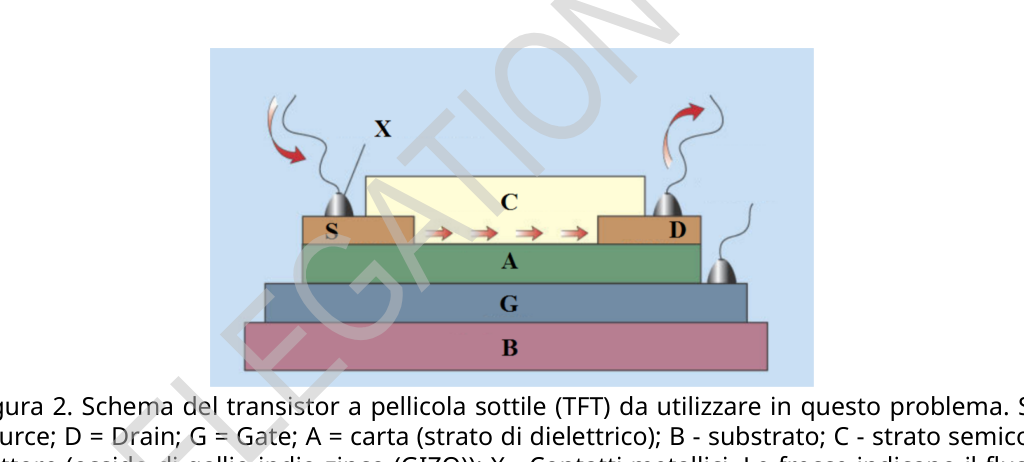
Experiment Q1-2 Italian (Italy) Dobbiamo sottolineare due caratteristiche molto importanti di un JFET. Sebbene la sua resistenza di uscita (controllata dalla tensione) possa essere molto bassa, la resistenza di ingresso (RGS = VGS/IGS) è estremamente alta, solitamente maggiore di 109 , quindi questo dispositivo utilizza pochissima corrente in ingresso. Inoltre, la capacità di un JFET di piccole dimensioni è piuttosto bassa, il che lo rende un dispositivo molto veloce che può ”aprirsi e chiudersi” con frequenze superiori al MHz. Ora procediamo a descrivere come funziona un diverso tipo di FET, il TFT. Come qualsiasi altro FET, il TFT consente il controllo di una corrente tra due contatti, gli elettrodi ”Drain” e ”Source”, mediante un potenziale applicato al terzo elettrodo, il Gate. L’elettrodo Gate è fisicamente separato dallo strato di semiconduttore attraverso un dielettrico che consente la creazione di un campo elettrico verticale che controlla i portatori di carica liberi presenti nel semiconduttore (effetto di campo). Lo strato di dielettrico può essere sostituito da una membrana elettrolitica come un foglio di carta in cui esistono ioni mobili (vedi figura 2) e in questo caso la tensione applicata al Gate spingerà gli ioni con carica opposta verso l’interfaccia del semiconduttore, creando uno strato di cariche ioniche che modificherà la densità dei portatori liberi di carica presenti all’interno del semiconduttore (Electrolye Gated Transistors - EGT). I ricercatori della ”Universidade Nova” di Lisbona, sono stati pionieri nel 2008 nello sviluppo del ”transistor cartaceo”, e sono leader mondiali in questo campo. Figura 2. Schema del transistor a pellicola sottile (TFT) da utilizzare in questo problema. S = Source; D = Drain; G = Gate; A = carta (strato di dielettrico); B - substrato; C - strato semiconduttore (ossido di gallio-indio-zinco (GIZO)); X - Contatti metallici. Le frecce indicano il flusso corrente. Analogamente ai JFET, i transistor TFT possono operare in due modalità operative fondamentali, una modalità lineare e una modalità di saturazione. Al contrario dei JFET, la capacità intrinseca dei TFT è un parametro rilevante per le prestazioni del dispositivo. In questo problema sperimentale ti si chiede di esaminare come funziona un JFET a canale n e un TFT cartaceo. Devi determinare le curve caratteristiche (CC) di questi dispositivi misurando la corrente tra Se D(IDS) attraverso l’applicazione di varie tensioni a G(VGS) e D(VDS). Le due CC più importanti sono le curve di output e di trasferimento: • Curva di output: per questa curva la corrente tra Source e Drain (IDS) verrà misurata e tracciata in funzione della tensione tra Source e Drain (VDS), lasciando variare VDSda 0 Vfino a +3 V , in passi successivi, mantenendo VGS costante.
Experiment Q1-3 Italian (Italy) • Curva di trasferimento: per questa curva, IDSsarà misurata e graficata come funzione di VGS. VDS verrà mantenuta costante con un valore appropriato in modo che il transistor funzioni in modalità di saturazione e VGSverrà fatto variare da Va 0 Vin passi successivi.
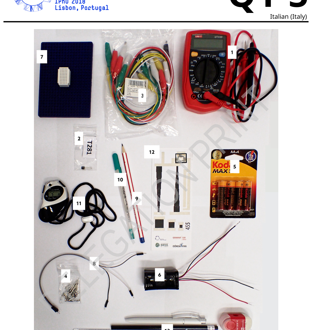
Experiment Q1-4 Italian (Italy) Materiale Il seguente materiale (Figura 3) è fornito per questo problema sperimentale:
- multimetro
- transistor JFET (fornito all’interno di una busta di plastica etichettata)
- cavi (10) con morsetti a coccodrillo
- morsetti a coccodrillo piatti (4, forniti all’interno di un sacchetto di plastica)
- batterie (4 1,5 V)
- portabatterie
- piastrina forata (mini-breadboard) con supporto
- cavetti sottili (3) per i collegamenti alla piastrina forata
- matita HB
- penna con inchiostro argentato conduttore (Circuit Scribe)
- cronometro
- foglio di carta con circuiti stampati e TFT incorporato che utilizza la carta come strato dielettrico (Figura 4)
- borsa con materiale di scrittura (1 penna, 1 matita, 1 gomma / temperino, 1 righello)
Experiment Q1-5 Italian (Italy) Figura 3. Materiale sperimentale
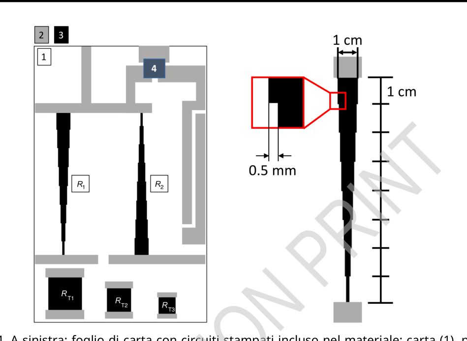
Experiment Q1-6 Italian (Italy) Figura 4. A sinistra: foglio di carta con circuiti stampati incluso nel materiale: carta (1), piste conduttrici argentate (2), piste resistive al carbonio (3), transistor di carta (4), resistenze del partitore di tensione (R1 e R2). A destra: dimensioni fisiche delle resistenze del partitore di tensione (i passi di 0,5 mm sono costanti per ciascun pezzo). Precauzione importante: Non piegare il foglio di carta con i circuiti stampati ed il transistor inserito poiché si potrebbe danneggiare. Cerca di lasciarlo il più possibile piatto durante le misure al fine di raggiungere i migliori risultati. Ai fini delle misure è importante considerare le seguenti importanti informazioni:
Experiment Q1-7 Italian (Italy) • Il multimetro deve operare sempre in modalità CD • Il multimetro non autoregola la portata e devi attentamente scegliere quelle più appropriate per le tue misure . Nel caso il valore sia fuori dall’intervallo delle letture , il display mostrerà ”1” o ”-1” (a sinistra del display) per valori
p.1 — Schema JFET, analogia idraulica e simbolo
p.2 — Schema TFT a effetto di campo
p.5 — Materiale sperimentale fornito
p.6 — Foglio circuiti stampati e dimensioni resistenze
p.8 — Partitore di tensione
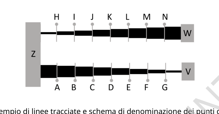
p.9 — Punti di contatto sulle linee tracciate
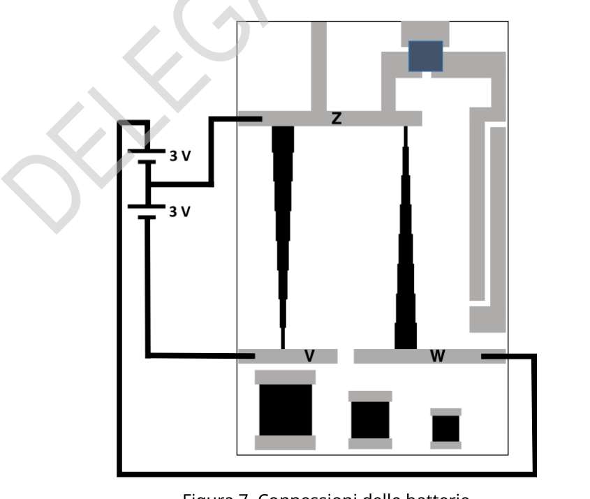
p.9 — Connessioni delle batterie
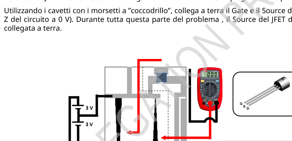
p.10 — Apparato caratterizzazione JFET e piedinatura
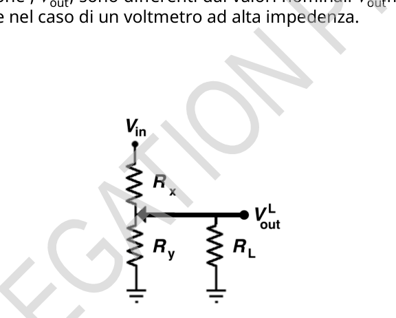
p.11 — Partitore di tensione con carico
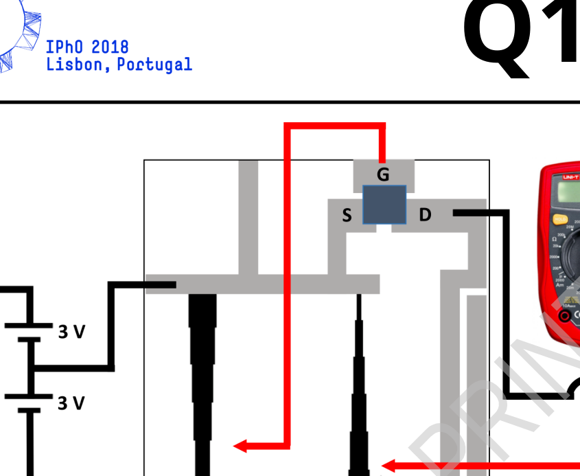
p.13 — Misura caratteristiche TFT
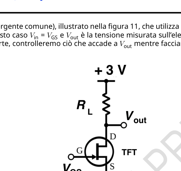
p.14 — Amplificatore a Source comune, circuito inverter
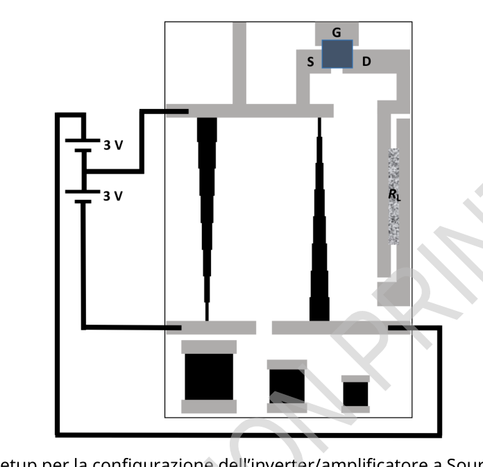
p.15 — Setup inverter/amplificatore a Source comune
Topic: Circuits, Electrostatics, Electromagnetism Metodi: Experimental Data Analysis, Kirchhoff’s Laws, Graph Linearization Competenze: Experimental Data Analysis, Measurement & Instrumentation, Graph Linearization Objects: Battery, Wire, Resistor Fonte: Testo (PDF) — p.1
Experiments Q1-1 Italian (Italy) The following table shows the calculation of the value of the input: The electronic technology in modern society is based on a simple but powerful device: the transistor, which can be used both as a switch and as an amplifier. In switch mode the The transistor is used for storing and processing digital information. Here we will analyze two types of field-effect transistors: the JFET (transistor) The test results shall be presented in accordance with the following conditions: Let’s briefly explain how a FET works. A FET is a non-linear device with 3 terminals [the terminals are called Base (Gate G); emitter (Source S); collector (Drain D) ] that can control the flow The current between Source and Drain acting on the voltage applied between Gate and Source . In a simple, though imperfect, analogy, a FET works similarly to a water tap, where the manoeuvre that is used is controls the flow of water plays a similar role to the Gate. Figure 1 is shown. Scheme of a JFET with channel n (left), its hydraulic analogy (center) and the the symbol of the electrical circuit (right). The arrows in the JFET diagram (Figure left) indicate the flow of electric current between Source (S) and Drain (D) through the narrow channel n. The channel width depends on the voltage applied between Gate (G) and Source (S). Junction-FET (JFET) works by the properties of the junction (contact) between two types of semiconductor material, such as p and n-duty silicon. For this reason it is called Junction-FET. Un JFET contains a narrow channel through which current flows between Source and Drain, and in a channel n FET this channel is made of n-type material. The width of this channel can be controlled in modo preciso applicando una tensione negativa tra Gate e Source, VGS= . For the purposes of this Regulation, the following: The current flowing between Source and Drain depends nonlinearly on the voltage applied between Drain e Source, VDS= . However, if the VDS voltage is small, the current depends linearly on the The JFET follows Ohm’s law. However, the output resistance, RDS=VDS Other It depends heavily on the applied VGS voltage, and follows the law closely: RDS = R0 DS 1 , (1) where R0 DS is the output resistance for VGS=0 and VP<0 is a JFET relative parameter called the voltage I’m not going to be a pinch-off. Clearly, at the pinch-off voltage, the FET completely blocks the current flow. For each fixed VGS> VP, the current between Source and Drain will begin to deviate from the linear behavior of increasing VDS, and at some point will reach saturation at an almost constant value. We call the IDSS the saturation current for VGS=0. In the saturation regime (i.e. for VDSgrande), The saturation current depends on the VGS as follows: IDS = IDSS (1 . (2)
Experiments Q1-2 Italian (Italy) We have to highlight two very important features of a JFET. Although its resistance to The output (controlled by the voltage) can be very low, the input resistance (RGS = VGS/IGS) is estremamente alta, solitamente maggiore di 109 , quindi questo dispositivo utilizza pochissima corrente in ingresso. In addition, the capacity of a small JFET is rather low, making it a A very fast device that can open and close at frequencies above MHz. Now let’s go on to describe how a different type of FET works, the TFT. Like any other FET, the TFT allows the control of a current between two contacts, the electrodes Drain and Source, by a potential applied to the third electrode, the Gate. The Gate electrode is physically separated from the semiconductor layer by a dielectric which allows the creation of a vertical electric field which controls the free charge carriers present in the gate. The test chemical shall be used to determine the concentration of the test chemical. The dielectric layer can be replaced by an electrolytic membrane such as a sheet of paper in which there are movable ions (see Figure 2) and in this case the voltage Applied to the Gate will push oppositely charged ions towards the semiconductor interface, creating a layer of ionic charge that will modify the density of the free charge carriers present inside The manufacturer shall ensure that the vehicle is equipped with a safety-guaranteed system. Researchers at the Universidade Nova in Lisbon, were pioneers in 2008 in the development of the paper transistor, and are world leaders in this field. The field. Figure two. The thin film transistor (TFT) scheme to be used in this problem. S = The following elements are added: source; D = drain; G = gate; A = paper (dielectric layer); B - substrate; C - semiconductor layer (gallium-Hindu-Zinc oxide (GIZO)); X - metal contacts. The arrows indicate the flow The current. Like JFETs, TFT transistors can operate in two basic operating modes, one linear mode and saturation mode. In contrast to JFETs, the intrinsic capacity of TFTs is a a parameter relevant to the device’s performance. In this experimental problem, you’re asked to examine how an n-channel JFET and a TFT work.
- It’s paper. You have to determine the characteristic curves (CC) of these devices by measuring the current between Se D(IDS) The application of various voltages to G(VGS) and D(VDS). The two most important CCs are the output and transfer curves: • Output curve: for this curve the current between Source and Drain (IDS) will be measured and traced in The voltage between Source and Drain (VDS) function, leaving VDS to vary from 0 V to +3 V, in steps the following, while keeping VGS constant.
Experiments Q1-3 Italian (Italy) • Transfer curve: for this curve, IDS will be measured and graphed as a function of VGS. VDS The transistor shall be kept constant at an appropriate value so that the transistor is operating in mode The VGS will be varied by V 0 Vin next steps.
Experiments Q1-4 Italian (Italy) Other materials The following material (Figure 3) is provided for this experimental problem:
- Multi-meter
- JFET transistor (provided inside a labelled plastic bag)
- Other, of a width of not more than 30 mm, but not more than 30 mm
- Plated crocodile seals (4, provided in a plastic bag)
- batterie (4 1,5 V)
- Other, of a kind used for the manufacture of motor vehicles
- a diameter of not more than 30 mm,
- Other, of a kind used for the manufacture of electrical equipment
- pencil HB
- a pen with a silver ink conductor (Circuit Scribe)
- The time-meter
- Paper with printed circuit board and TFT incorporated, using paper as a dielectric layer (Figure 4)
- Bag with writing material (1 pen, 1 pencil, 1 rubber/tinder, 1 ruler)
Experiments Q1-5 Italian (Italy) Figure 3 is shown. Testing material
Experiments Q1-6 Italian (Italy) Figure 4 is shown. Left: sheet of paper with printed circuit boards included in the material: paper (1), tracks Silver conductors (2), carbon resistant tracks (3), paper transistors (4), The voltage score (R1 and R2) shall be determined by the following: Right: physical dimensions of the resistance of the scorer of The voltage (the steps of 0,5 mm are constant for each piece). Important precautions: Do not fold the paper with the printed circuit board and the inserted transistor as it may be damaged. Try to leave it as flat as possible during the measurements in order to reach the best The results. For the purposes of the measures, it is important to consider the following important information:
Experiments Q1-7 Italian (Italy) • The multimeter must always operate in CD mode • The multimeter does not self-regulate the range and you must carefully choose the most appropriate ones For your measurements . If the value is outside the read range , the display will display 1 or -1 (left of the display) for values
p.1 — Schema JFET, analogia idraulica e simbolo
p.2 — Schema TFT a effetto di campo
p.5 — Materiale sperimentale fornito
**p.6 ** Paper printed circuit boards and resistance sizes
p.8 — Partitore di tensione
p.9 — Punti di contatto sulle linee tracciate
p.9 — Connessioni delle batterie
p.10 — Apparato caratterizzazione JFET e piedinatura
p.11 — Partitore di tensione con carico
p.13 — Misura caratteristiche TFT
p.14 — Amplificatore a Source comune, circuito inverter
p.15 — Setup inverter/amplificatore a Source comune
Topic: Circuits, Electrostatics, Electromagnetism Metodi: Experimental Data Analysis, Kirchhoff’s Laws, Graph Linearization Competenze: Experimental Data Analysis, Measurement & Instrumentation, Graph Linearization Objects: Battery, Wire, Resistor Fonte: Testo (PDF) — p.1